


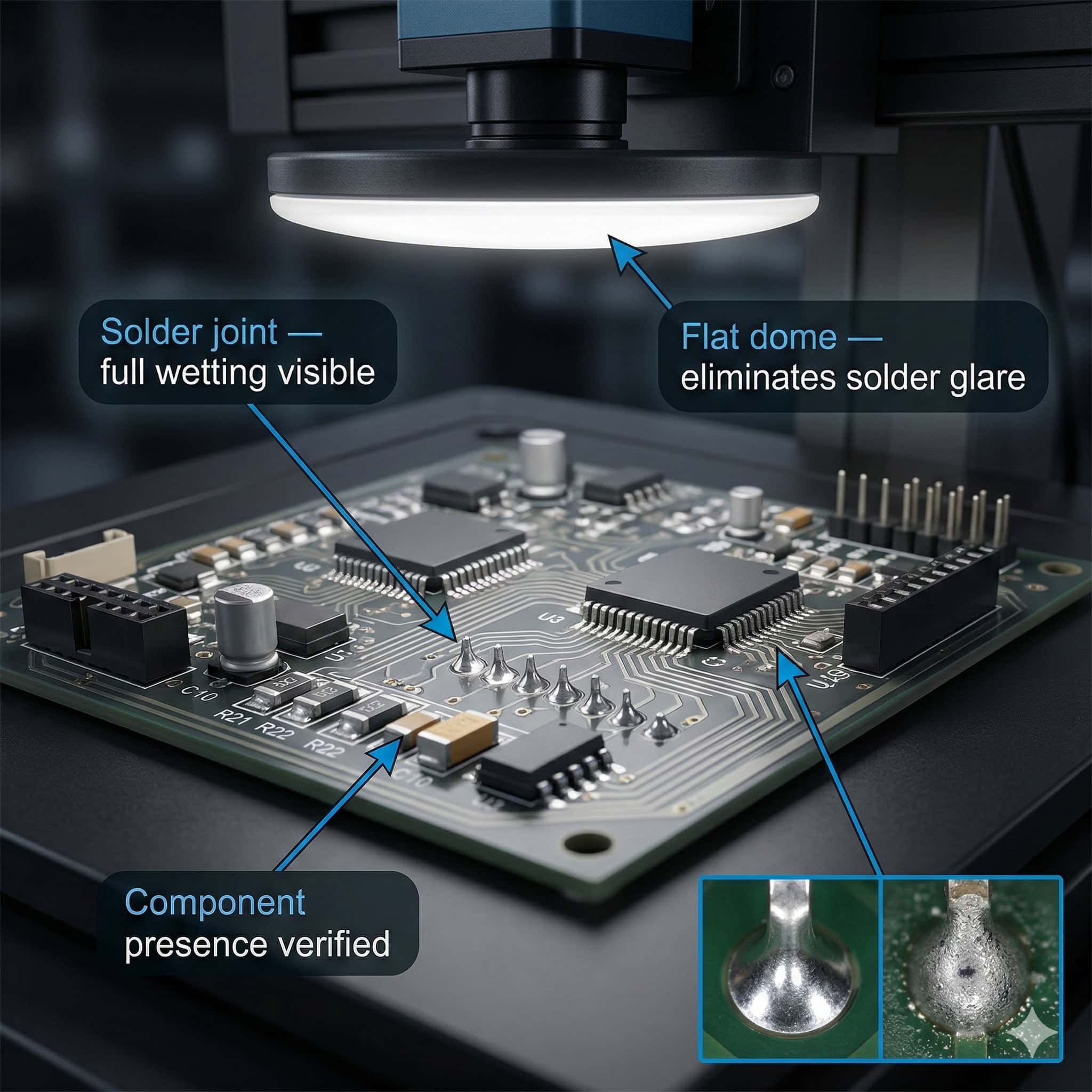
PCB and electronics inspection ranks among the most demanding applications in industrial machine vision. Component dimensions shrink with every product generation. Solder joints are often smaller than 0.5 mm. Gold-plated pads, tin-coated surfaces, and solder paste all carry very different reflectance properties. An illumination approach that works for one task on a PCB can produce completely unusable images for another task on the same board.
The illumination engineer therefore has to treat PCB inspection as a multi-task problem. Different inspection tasks call for different illumination geometries, often on the same board in the same production line. Understanding the optical characteristics of each inspection target is the starting point for designing an effective illumination strategy.
The PCB Inspection Challenge: Miniaturisation and Reflective Surfaces
Modern PCBs pack multiple surface types into a very small area. Bare FR4 substrate, solder mask, solder paste, solder joints, copper traces, gold-plated pads, component bodies, component markings, and adhesive dots may all sit within a few square centimetres. Each material carries a different reflectance, colour, and surface texture, and each responds differently to direct, diffuse, coaxial, and darkfield illumination.
The drive toward miniaturisation sharpens the problem. As component packages shrink from QFP to BGA to CSP, the spatial resolution the inspection system needs climbs. Higher magnification means a smaller field of view, which in turn means the illuminator has to deliver consistent intensity and uniformity over a smaller area while holding the correct geometry for the inspection task.

Do you want help choosing the product?
Solder Joint Inspection: Coaxial and Dark-Field Illumination
Solder joint inspection is the most critical task in SMT assembly quality control. The aim is to catch insufficient solder, excess solder, solder bridges, cold joints, and tombstoning. Each defect type carries a different three-dimensional form and a different optical signature.
Coaxial Illumination for Flat Solder Surfaces
Well-formed solder joints on flat pads have a characteristic mirror-like flat top surface. Coaxial illumination—where the light travels along the optical axis of the camera—produces a bright, uniform reflection from this flat surface. Defective joints with a rough, irregular, or tilted surface bounce less light back along the optical axis and read darker. That brightness difference is the basis for coaxial solder joint inspection.
Coaxial illumination also works well for inspecting gold-plated pads before soldering. The gold surface is highly specular, so under coaxial illumination gold pads read uniformly bright. Contamination, oxidation, or damage on the pad surface breaks the specular reflection and reads as a darker region. That allows pre-reflow pad inspection as well as solder joint quality verification.
Dark-Field Illumination for Solder Defect Detection
Darkfield illumination at low angles works well for catching solder bridges, solder balls, and surface contamination on PCBs. Under grazing-incidence illumination, the flat solder mask and flat pad surfaces read dark. Raised solder features—bridges between pads, solder balls on the board surface, lifted component leads—scatter light and read bright. That contrast makes small solder defects visible even when they are only a fraction of a millimetre high.
Component Placement Verification: Backlight and Ring Illumination
Component placement verification checks that components are present, correctly oriented, and within placement tolerance. Different component types call for different illumination approaches.
Backlight for Leaded Component Outline Inspection
For leaded through-hole components and large SMT packages with visible lead outlines, backlight illumination gives the highest contrast for lead position and bend measurement. The component leads read as dark silhouettes against the bright backlight. Coplanarity of leads, lead spacing, and the presence of bent or missing leads are all measurable from the silhouette image with sub-pixel accuracy.
Ring Illumination for Component Presence and Polarity
Ring illuminators give front illumination well suited to component presence detection and polarity marking reading. The ring geometry lights the top surface of the component from all azimuths, producing a uniform bright-field image of the component body. Component markings, polarity indicators, and orientation features stand out against the component body background. This is the standard approach for confirming correct orientation of diodes, electrolytic capacitors, and polarised ICs.
Trace and Via Inspection on Bare Boards
Bare board inspection checks copper trace continuity, trace width, trace spacing, and via presence before components are mounted. The inspection target is the copper trace pattern on the solder mask surface.
Coaxial or near-coaxial direct illumination is the standard approach for bare board inspection. The solder mask surface has a defined reflectance, and the copper trace areas have a different one. The contrast between the two lets the trace pattern be imaged clearly. For high-density boards with very fine trace widths below 100 micrometres, NIR illumination can sharpen the contrast between copper and solder mask by drawing on the different spectral reflectance of the two materials.
Via Inspection
Via holes on a bare board read as dark circles against the bright surrounding copper or solder mask under coaxial illumination. The via diameter, spacing, and fill status are measurable from the image. Unfilled vias that should have been plated look different from properly filled vias. Backlight illumination can also serve via inspection when the board is thin enough for light transmission.
IC Marking and Serialisation Reading
IC marking verification and datamatrix or barcode reading on component packages are common tasks in electronics inspection. The marking is usually laser-etched or ink-printed on a plastic or ceramic package body. The contrast between the marking and the package surface depends on the marking type, package colour, and illumination conditions.
For laser-etched markings on dark IC packages, low-angle direct illumination lifts the height difference between the etched and unetched surface, giving better contrast than front-facing illumination. For ink-printed markings on plastic packages, direct front illumination at a moderate angle is usually enough. For data matrix codes that have to be read reliably at high speed, adequate intensity and the correct angle matter more than the specific illuminator geometry.
Handling Reflective Gold and Tin Surfaces Without Glare
Gold-plated connectors, tin-coated leads, and solder-wetted surfaces are among the most challenging materials in PCB inspection because of their very high specular reflectance. Under direct front illumination, these surfaces throw intense specular hotspots that saturate the camera sensor and hide the features of interest.
Three approaches are used to manage specular reflections from gold and tin surfaces.
The first is coaxial illumination, which uses the specular reflection constructively by lining the reflection up with the camera axis. Features that are flat and perpendicular to the optical axis read uniformly bright; features that are tilted or irregular read darker.
The second is dome or flat dome illumination, which fills the hemisphere of illumination angles so that specular reflections spread over the entire dome interior rather than concentrating at a single angle. That clears bright hotspots at the cost of some reduction in feature contrast.
The third is polarisation. A polarising filter on the illuminator and a cross-polarised analyser on the camera lens clear specular reflections from metallic surfaces. Only the diffusely scattered component of the reflected light passes through the cross-polarised analyser. That completely removes glare from gold and tin surfaces and reveals surface features masked by the specular reflection under unpolarised illumination.
Products and Technologies
RODER Vision Illuminator Families for PCB and Electronics Inspection
The RODER Vision product families below tackle the most common illumination needs in PCB assembly inspection and electronics quality control.

DC6 — High Density LED Ring
Ring illumination for component presence, polarity marking, solder joint inspection. Near-coaxial geometry for reflective pad surfaces. Multi-wavelength.

FD2 — Flat Dome LED Illuminators
Diffuse illumination for assembled PCBs with mixed reflective and matt surfaces. Clears specular hotspots. Ideal for full-board presence and cosmetic checks.

DL6 — High Density LED Matrix
Direct matrix illumination for bare board trace inspection, IC marking reading, and datamatrix verification. HTTM thermal stability. NIR and UV options.

BL3 — LED Backlight Series
Backlight for leaded component silhouette inspection: lead coplanarity, spacing, and bend detection. High uniformity. Multiple sizes and wavelengths.
Frequently Asked Questions
Coaxial illumination is the most effective technique for inspecting flat solder pad surfaces and gold-plated pads. It produces a bright, uniform reflection from flat surfaces and shows defects as darker regions. Darkfield illumination at low angles works well for catching raised solder defects such as bridges, solder balls, and lifted leads, which read bright against the dark background.
Three approaches are used: coaxial illumination, which uses the specular reflection constructively; dome or flat dome illumination, which spreads reflections across the entire hemisphere to clear hotspots; and cross-polarised illumination, which removes specular reflections entirely with a polarising filter on the illuminator and a cross-polarised analyser on the camera lens. Cross-polarisation is the most complete way to clear glare from gold and tin surfaces.
NIR wavelengths (850 nm or 940 nm) can sharpen the contrast between copper traces and solder mask on bare boards by drawing on the different spectral reflectance of the two materials. UV illumination can lift the contrast of certain solder mask colours and reveal contamination on pad surfaces. For general PCB inspection, red (617 nm) or white illumination is a good starting point, with NIR or UV considered where standard visible wavelengths fall short on contrast.
In most cases, different inspection tasks on the same PCB call for different illumination geometries. A single camera station may use a ring illuminator for component presence and a flat dome for assembled board cosmetic inspection, triggered separately for each task. For high-throughput inline AOI systems, several illumination modes are triggered in sequence to capture separate images for each task at full production speed.
For laser-etched datamatrix codes on dark IC packages, low-angle direct illumination lifts the height difference between etched and unetched areas, improving contrast. For ink-printed codes, front-facing direct illumination at a moderate angle is usually enough. Adequate intensity and the correct angle matter more than the specific illuminator geometry. Strobe mode delivers enough intensity without thermal degradation of the illuminator.
Contacts & Information
Contact for general information : info@roder.it
Systems and Sensor Integration Partner : www.roder.it
RODER Artificial Vision Division : www.rodervision.com
RODER Instruments Division : www.innovacheck.com
More information about RODER VISION : about us
The information on this website is provided for informational purposes only. Although it has been prepared with the utmost care, it does not constitute a contractual offer or a binding commitment to supply. It may contain transcription, translation, or typographical errors. For precise and up-to-date information, please contact our company directly.
Please note: Some images on this website have been intentionally generated using Artificial Intelligence (AI). This is due to the fact that, for many applications and projects, it is not possible to disclose photographs of the actual installation or system due to confidentiality agreements, contractual clauses, and Non-Disclosure Agreements (NDAs).
